3.7 KiB
Developer Documentation
Hardware
Test Points
The PT100 PCB has 15 test points, numbered T1 to T15.
NOTE: T1, T2, T4, T5, T6, T7, T8, T9, T10, T11 are referenced to GND (T3). T4, T5, T6, T7, T8, T9, T10, T11 are 3.3V level signals.
NOTE: T12, T13, T15 are referenced to GNDISO (T14). T12, T13, T15 are 5V level signals.
-
T1 -
5V- USB 5V DC power rail
- Used for MCU USB circuitry and digital isolator power supply
-
T2 -
3V3- Regulated 3.3V DC power rail
- Used for MCU core/ports and EEPROM
-
T3 -
GND- Ground for PC connected circuitry (MCU/EEPROM)
-
T4 -
SBWTDIO- MCU debug/programming interface, connects to SBW RST on TI LaunchPad ez-FET header
-
T5 -
SBWTCK- MCU debug/programming interface, connects to SBW TST on TI LaunchPad ez-FET header
-
T6 -
GPIO1- General purpose I/O for debugging, pin P4.4 on MCU, hardware serial port on MCU (TX)
- Currently outputs a LOW when interrupts are enabled, and outputs a HIGH when interrupts are disabled (during reception of byte during timer operation)
-
T7 -
GPIO2- General purpose I/O for debugging, pin P4.5 on MCU, hardware serial port on MCU (RX)
- Currently toggles state when the
MCU_DATA_IN_3V3signal is being sampled
-
T8 -
MCU_DATA_OUT_3V3- Controls transistor for DATA signal
MCU_DATA_OUT_3V3LOW = transistor off = DATA line pulled HIGH (5VISO) by pull up resistorMCU_DATA_OUT_3V3HIGH = transistor on = DATA line pulled LOW (GNDISO) by transistor
-
T9 -
MCU_DATA_IN_3V3- Level shifted version of
KFD_DATA_IN
- Level shifted version of
-
T10 -
MCU_SENSE_OUT_3V3- Controls transistor for SENSE signal
MCU_SENSE_OUT_3V3LOW = transistor off = SENSE line pulled HIGH (5VISO) by pull up resistorMCU_SENSE_OUT_3V3HIGH = transistor on = SENSE line pulled LOW (GNDISO) by transistor
-
T11 -
MCU_SENSE_IN_3V3- Level shifted version of
KFD_SENSE_IN
- Level shifted version of
-
T12 -
KFD_DATA_IN- Target DATA signal
-
T13 -
KFD_SENSE_IN- Target SENSE signal
-
T14 -
GNDISO- Target isolated ground
-
T15 -
5VISO- Target isolated 5V DC power rail
External Logic Analyzer
A external logic analyzer can be connected to monitor the TWI signals independent of the KFDtool. The TWI physical protocol is close to a UART signal, and therefore UART protocol decoders of logic analyzers can be used.
There is no stop bit in the TWI protocol, where a stop bit is part of the UART protocol. The logic analyzer reports a framing error where it expects a stop bit, however this can be safely ignored.
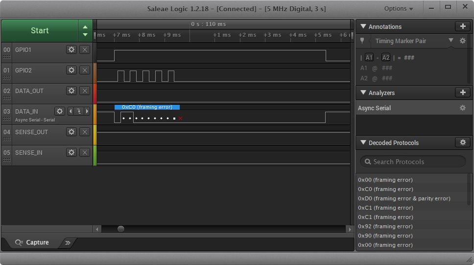
The following screenshots are of the Saleae logic analyzer software.
- Ground - connected to T3
- Channel 00 "GPIO1" - connected to T6
- Channel 01 "GPIO2" - connected to T7
- Channel 02 "DATA_OUT" - connected to T8
- Channel 03 "DATA_IN" - connected to T9
- Channel 04 "SENSE_OUT" - connected to T10
- Channel 05 "SENSE_IN" - connected to T11
- Trigger - Channel 03 "DATA_IN" falling edge
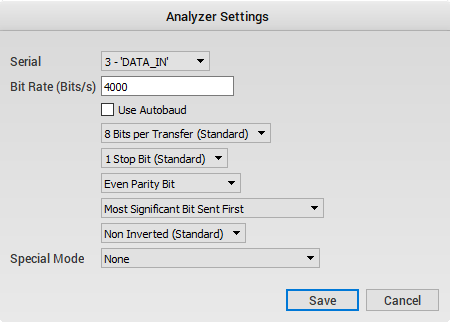
Async serial (UART) analyzer settings:
Firmware
Development/Build Environment
Firmware is built using TI CCS 9.
Software
Development/Build Environment
Software is built with Microsoft Visual Studio 2019.
Command Line
The KFDtoolCmd.exe program contains command line utilities. The following utilities are available:
-
read
- Description: Read bytes from the TWI interface
- Usage:
-read -port COM#
-
create
- Description: Create a firmware update package
- Usage:
-create -input generate.xml -output package - Example: generate.xml

